It can be seen that the one clock delay is implemented using a DFF and the output of the flip flop is wired to the input of an AND gate through an inverter. Esegue un programma ed elabora i segnali digitali ed analogici provenienti da sensori e diretti agli attuatori presenti in un impianto industriale con la struttura del PLC che viene.
Setting Up The Fpga Development Toolchain Imperix
Note that the inputs in the circuit here become the reg datatypes and the outputs are specified as wireThe reg data object holds its value from one procedural assignment statement to the next.

. Full_Subtractor_3 Instance0 D B X Y Z. A continuous assignment statement assigns values to the wire datatype and makes a connection to an. Reg X Y Z.
Il controllore logico programmabile in inglese programmable logic controller spesso in sigla PLC è un computer per lindustria specializzato in origine nella gestione o controllo dei processi industriali. Wire D B. The behavioral model in Verilog was synthesized using Xilinx Vivado FPGA design tool and the hardware schematic has been generated as shown below.
These digital elements are substituted with logical cells that belong to a.
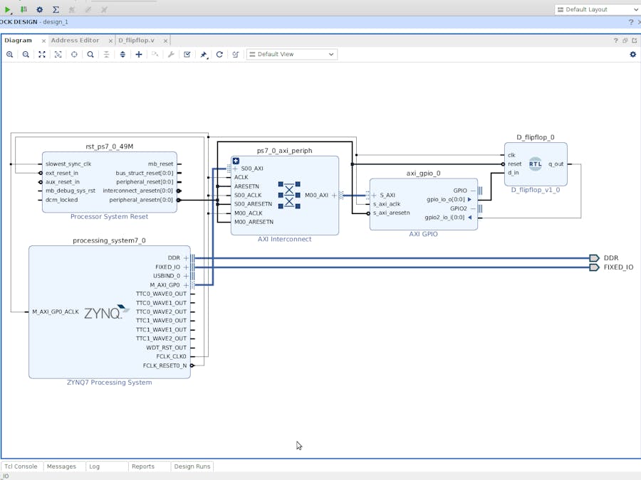
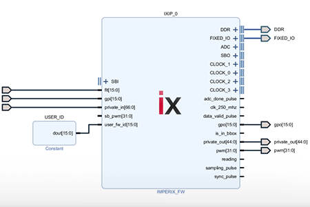
Add Custom Ip Modules To Vivado Block Design Hackster Io

Xilinx Vivado Block Design For Motor Emulator System Download Scientific Diagram
2
1 Depict The Vivado Block Diagram Of The Reference Design Developed In Download Scientific Diagram
2
Xilinx Vivado Block Design For Motor Emulator System Download Scientific Diagram
2

5 Pwm Ip Block Interconnections In Vivado Download Scientific Diagram
0 comments
Post a Comment